
Nanodevice and Materials Engineering
Semiconductors are used not only in computers, but also in various other places, such as solar cells, thermoelectric conversion devices and other power generation elements, and sensors that sense temperature and light. In addition to silicon, which is widely used today, our research targets new semiconductor materials with mechanical flexibility and excellent electrical properties, such as carbon nanotubes and semiconductive nanosheets, and we are conducting a series of research from structural control and design at the nanoscale (one billionth of a meter) to practical scale. We also perform research on defect properties and engineering in semiconducting materials.
 |
|
|---|---|
 |
|
 |
|
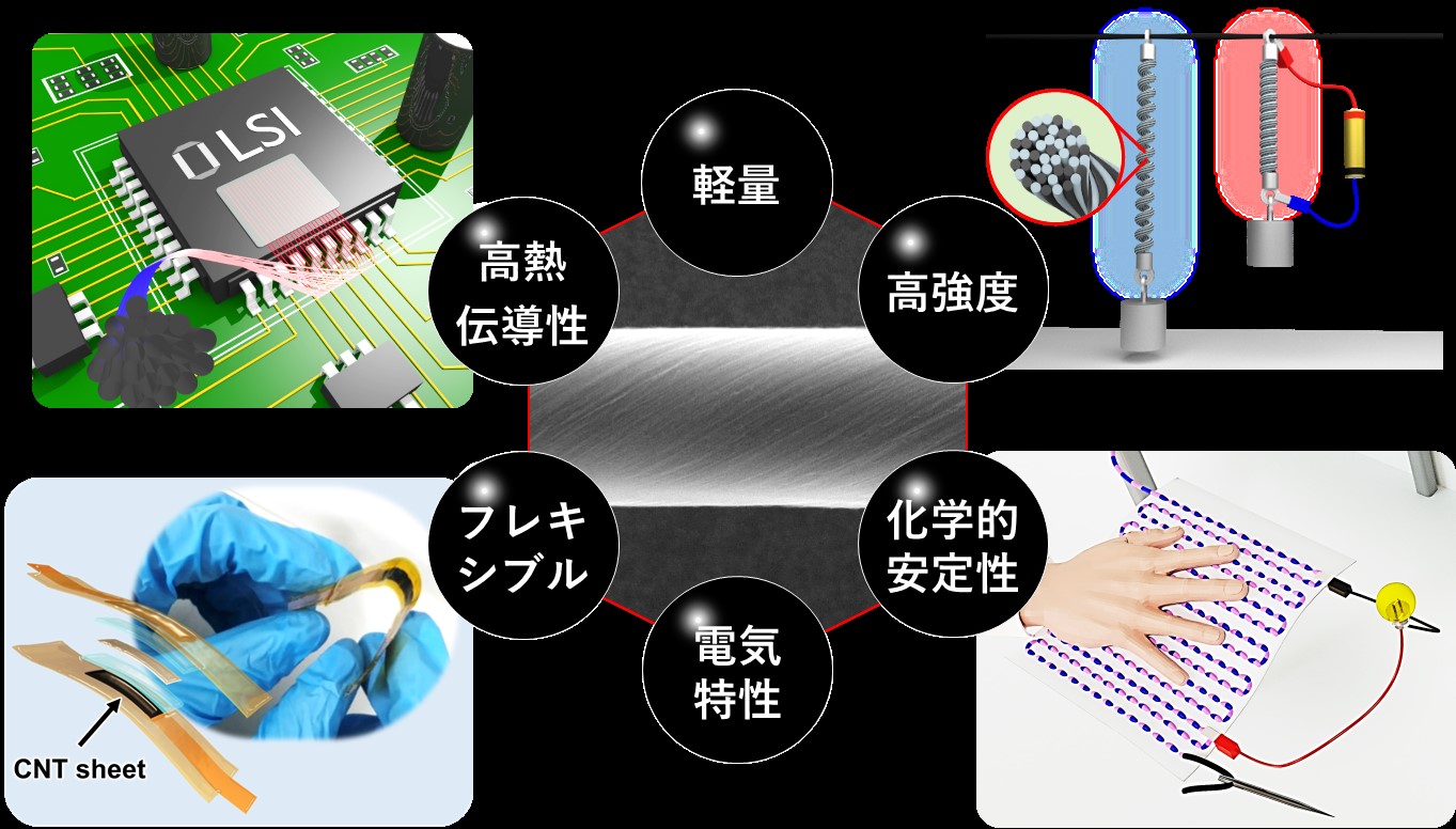
Carbon nanotubes are nanomaterials with mechanical flexibility and excellent electrical properties. Carbon nanotubes can be applied to energy harvesting devices and high strength wires. Based on our controlled growth technology to precisely control the structure of carbon nanotubes, we are attempting to improve the device performance by designing materials on the atomic scale. We aim to solve social problems such as environmental issues, welfare, and medicine by developing innovative nanodevices using carbon nanotubes.
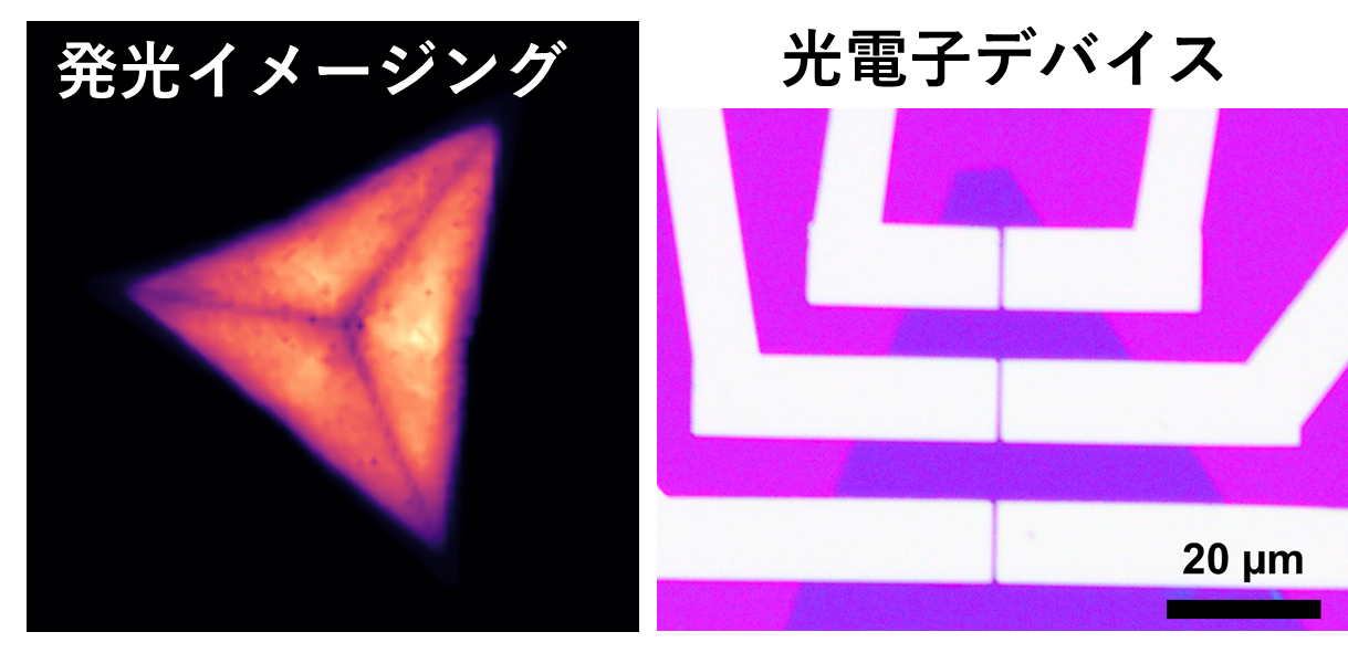
Semiconducting materials with an atomic thickness are called two-dimensional (2D) semiconductors. 2D semiconductors have the potential to be a new alternative to silicon. We are investigating growth methods of high quality 2D semiconductors such as transition metal dichalcogenides and controlling their structures at the atomic level for their applications in optoelectronic devices.
 |
|
|---|
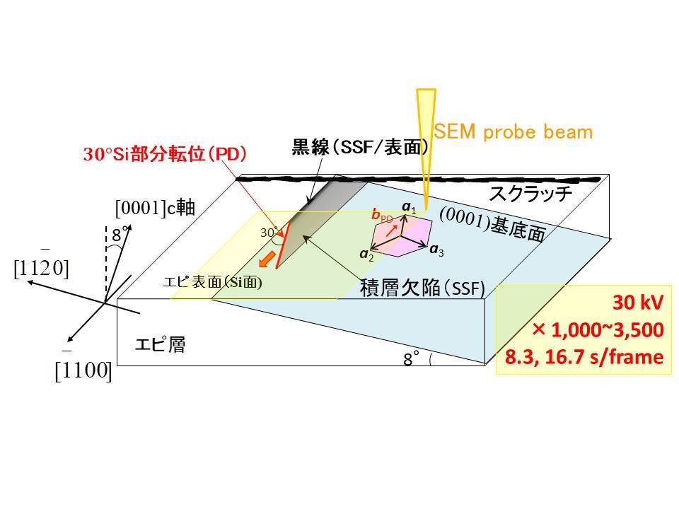
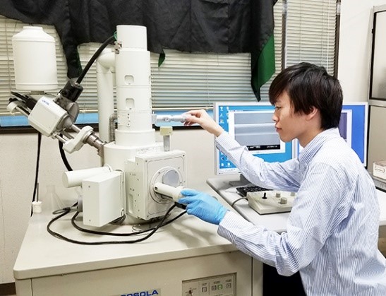
Silicon carbide, a power semiconductor material, is being put to practical use, but the generation of stacking faults during forward current operation is a major problem. We have been studying the motion of partial dislocations under electron excitation, which governs this phenomenon, using scanning electron microscopy to elucidate their properties from the level of elementary processes of dislocation motion.